Selected designR = 10 µmSOI microring
Projects
Computational Photonics Projects
Selected computational work focused on reproducible numerical modeling, integrated photonic devices, and physics-based design workflows.
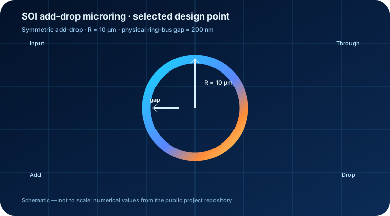
R = 10 µmgap = 200 nmMODE / varFDTD
Ring–bus gap200 nmValidated design point
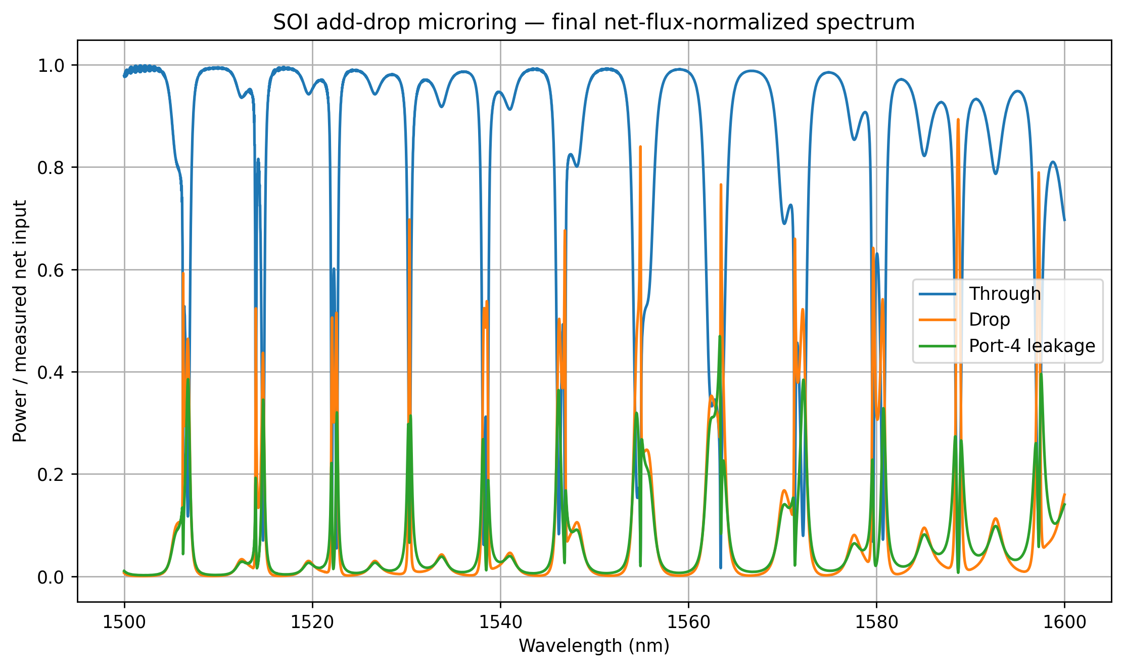
Median FSR8.00455 nmFinal spectrum
Median loaded Q2215.37varFDTD estimate
Selected Project
Featured computational project
A convergence-validated computational integrated-photonics workflow progressing from an SOI strip-waveguide model through dispersion analysis, bend-radius characterization, coupling-gap pre-screening, and full add-drop microring simulation.
Computational Integrated Photonics
Reproducible SOI Add-Drop Microring Resonator
The project uses Ansys Lumerical MODE / varFDTD with Python automation through lumapi to build and validate a reproducible SOI microring-resonator simulation workflow.
SOI
MODE / varFDTD
Python
lumapi
Final Design Point
Selected numerical results
- Ring radius
- 10 µm
- Ring–bus gap
- 200 nm
- Median FSR
- 8.00455 nm
- Median loaded Q
- 2215.37
- Median extinction
- 11.79 dB
- Spectrum samples
- 4001
Workflow
Reproducible simulation progression
 01
01SOI strip-waveguide baseline
Establish the fundamental waveguide model and characterize the guided mode.
 02
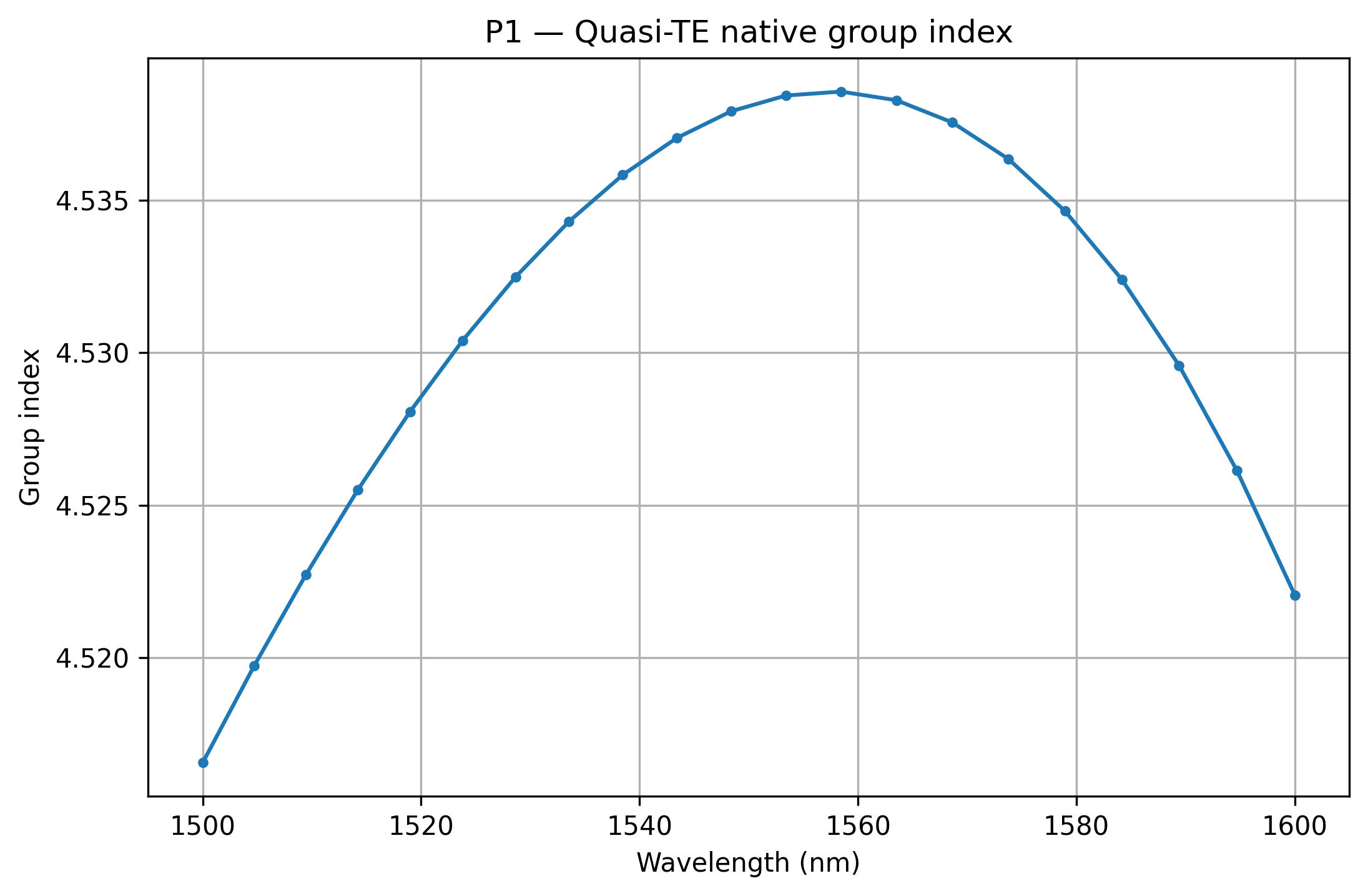
02Convergence and dispersion
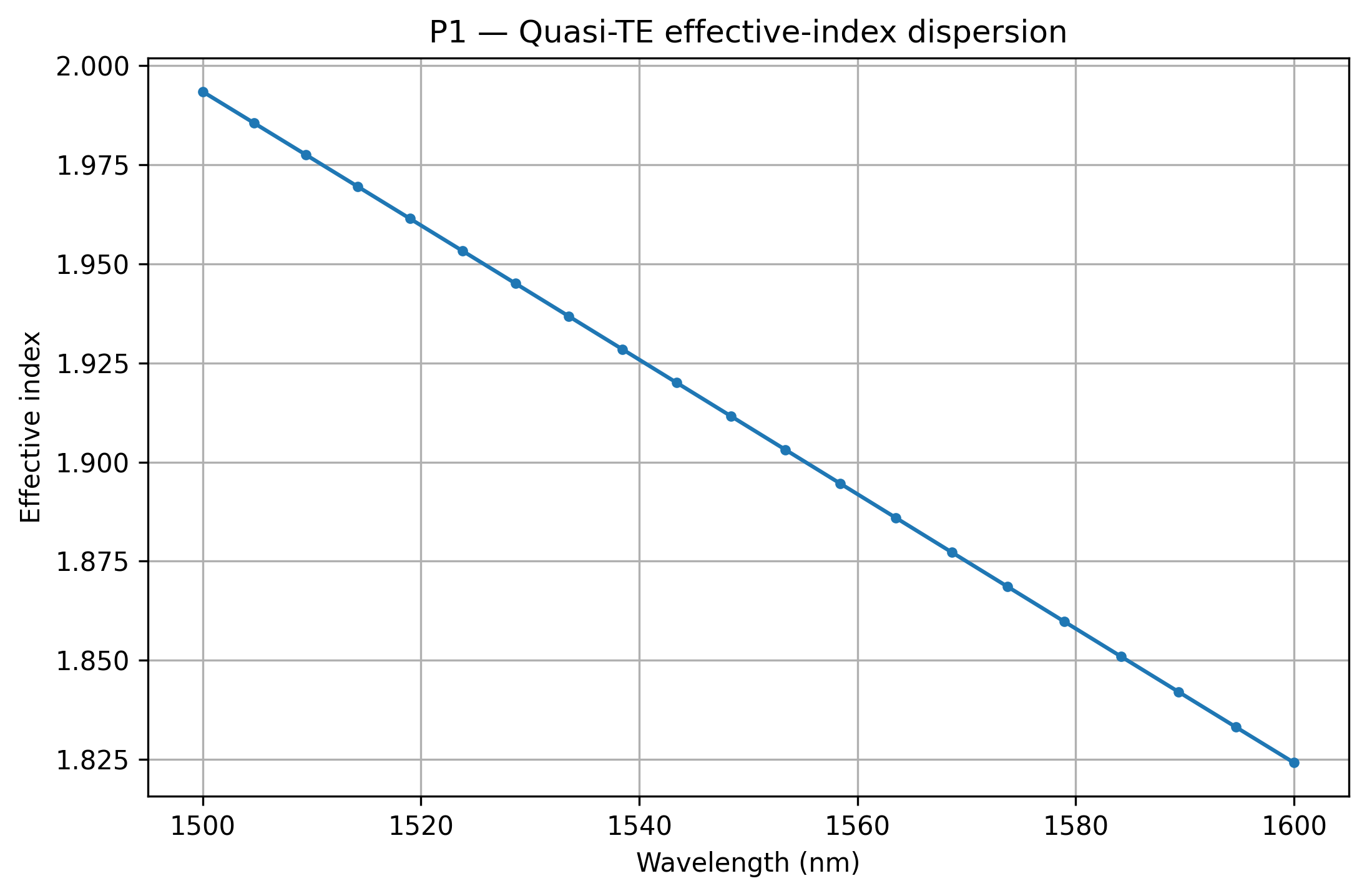
Evaluate domain and mesh convergence, effective index, group index, and wavelength-dependent behavior.
 03
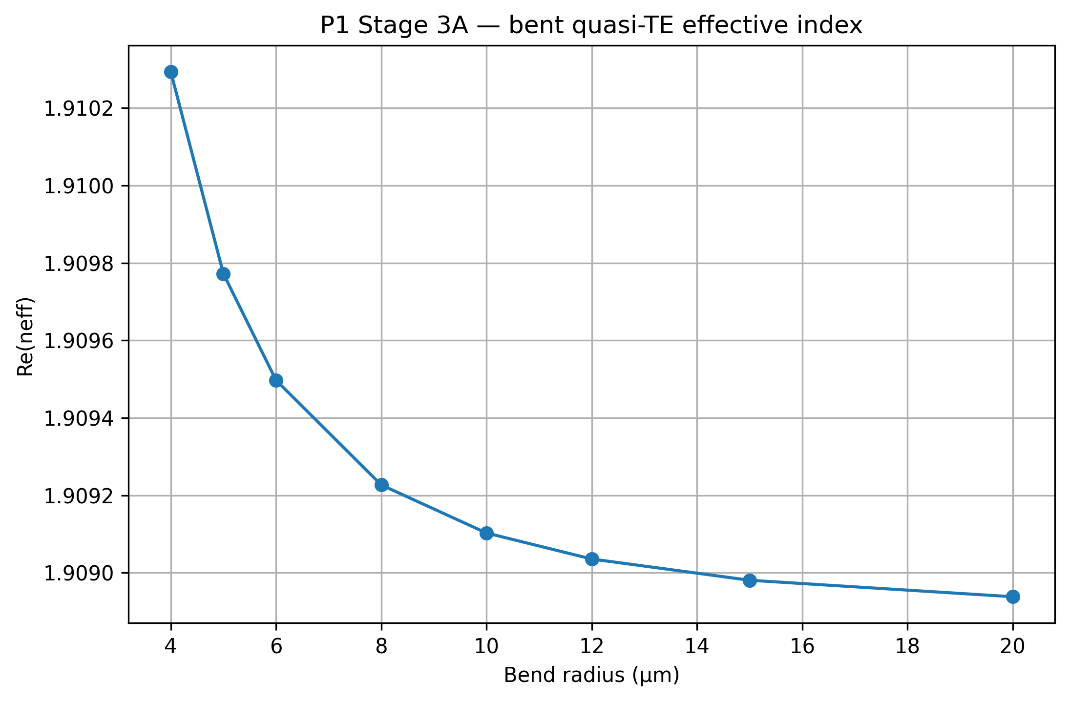
03Bend and coupling characterization
Characterize bend radius and use straight-coupler supermode analysis as a gap pre-screen.
- 04
Full add-drop microring model
Simulate the complete symmetric add-drop resonator using varFDTD at the selected design point.
- 05
Validation and refinement
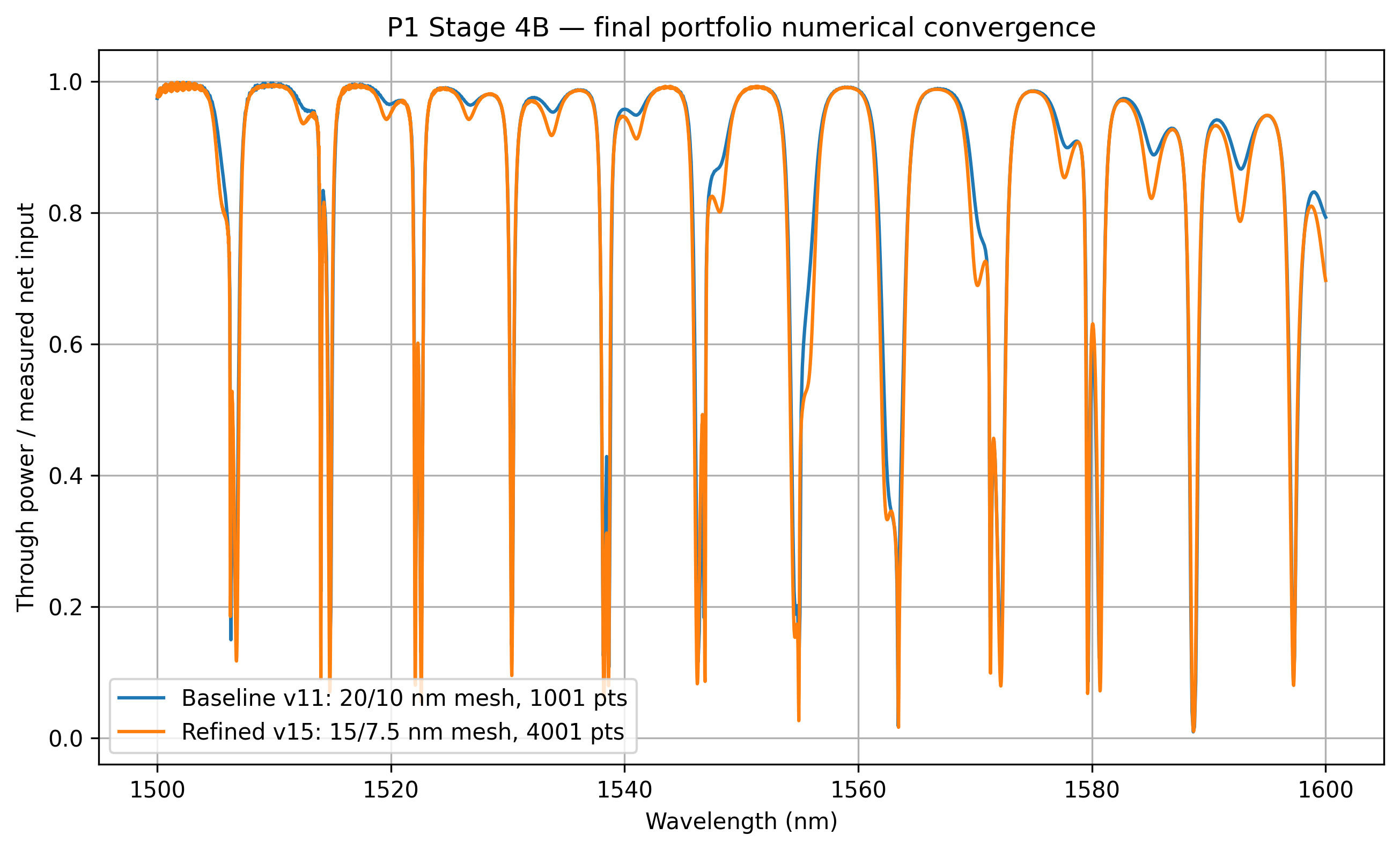
Check time-decay behavior, net-flux normalization, mesh refinement, and spectral refinement.
- 06
Resonance metrics
Extract FSR, loaded Q, extinction ratio, and the final resonance dataset.
Scope
What this project demonstrates
This project demonstrates a reproducible computational workflow for integrated-photonic device modeling and numerical validation using MODE / varFDTD and Python automation.
The current release does not claim full 3D-FDTD validation, fabrication, or experimental verification. The selected 200 nm coupling gap is a validated design point within the reported model, not a claim of global optimality.